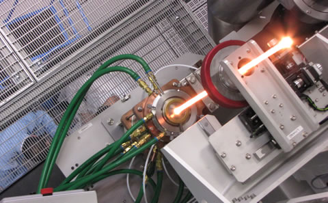
Focused Ion Beam

The focused ion beam facility (FIB) specialises in rapid nanostructuring of metallic, semiconducting and dielectric materials and devices, from free-standing nanomembranes to multilayer structures and optical fibres for nanophotonics/electronics, metamaterials and plasmonics research. Our two gallium FIB systems provide milling resolution down to 30nm, and additional capabilities including high-resolution electron microscopy and electron beam lithography, beam-induced deposition of platinum, tungsten, carbon and silicon dioxide, and chemically accelerated milling of insulators, all on substrates up to 150mm in diameter. The Helium Ion Microscope provides FIB milling at even smaller scales, enabling precise material modification in the sub-10nm range.
Achievements
An essential and highly flexible prototyping tool enabling numerous ground-breaking devices and discoveries including:
- Realising the first reconfigurable photonic metamaterials for the optical part of the spectrum – devices harnessing elastic, electrostatic, magnetic and even optical forces on the nanoscale to deliver dynamically controllable optical functionalities on demand.
- Fabricating optical fibre probes to interrogate and even amplify the evanescent field of free-flying electrons and new superconducting metamaterial technologies for modulating and detecting sub-terahertz radiation.
- Demonstrating Microfibre Bragg gratings and whispering gallery mode selection demonstrated in optical bottle micro-resonators and observing novel phenomena in nanophotonic architectures.
Facility contact
Contact us to discuss how you can access our facilities for research and development projects.
Equipment
Click to view the FIB equipment list